Beyond Moore’s Law: taking transistor arrays into the third dimension
Thin film transistors stacked on top of a state-of-the-art silicon chip could help shrink electronics while improving performance.

 Enlarge
Silicon integrated circuits, which are used in computer processors, are approaching the maximum feasible density of transistors on a single chip—at least, in two-dimensional arrays. Now, a team of engineers at the University of Michigan have stacked a second layer of transistors directly atop a state-of-the-art silicon chip.
They propose that their design could remove the need for a second chip that converts between high and low voltage signals, which currently stands between the low voltage processing chips and the higher voltage user interfaces.
“Our approach can achieve better performance in a smaller, lighter package,” said Becky Peterson, an associate professor of electrical engineering and computer science and project leader.
Moore’s Law holds that computing power per dollar doubles roughly every two years. As silicon transistors have shrunk in size to become more affordable and power efficient, the voltages at which they operate have also fallen. Higher voltages would damage the increasingly small transistors. Because of this, state-of-the-art processing chips aren’t compatible with higher-voltage user interface components, such as touchpads and display drivers. These need to run at higher voltages to avoid effects such as false touch signals or too-low brightness settings.
“To solve this problem, we’re integrating different types of devices with silicon circuits in 3D, and those devices allow you to do things that the silicon transistors can’t do,” said Peterson.
Because the second layer of transistors can handle higher voltages, they essentially give each silicon transistor its own interpreter for talking to the outside world. This gets around the current trade-off of using state-of-the-art processors with an extra chip to convert signals between the processor and interface devices—or using a lower-grade processor that runs at a higher voltage.
“This enables a more compact chip with more functionality than what is possible with only silicon,” said Youngbae Son, the first author of the paper and recent PhD graduate in electrical and computer engineering at U-M.
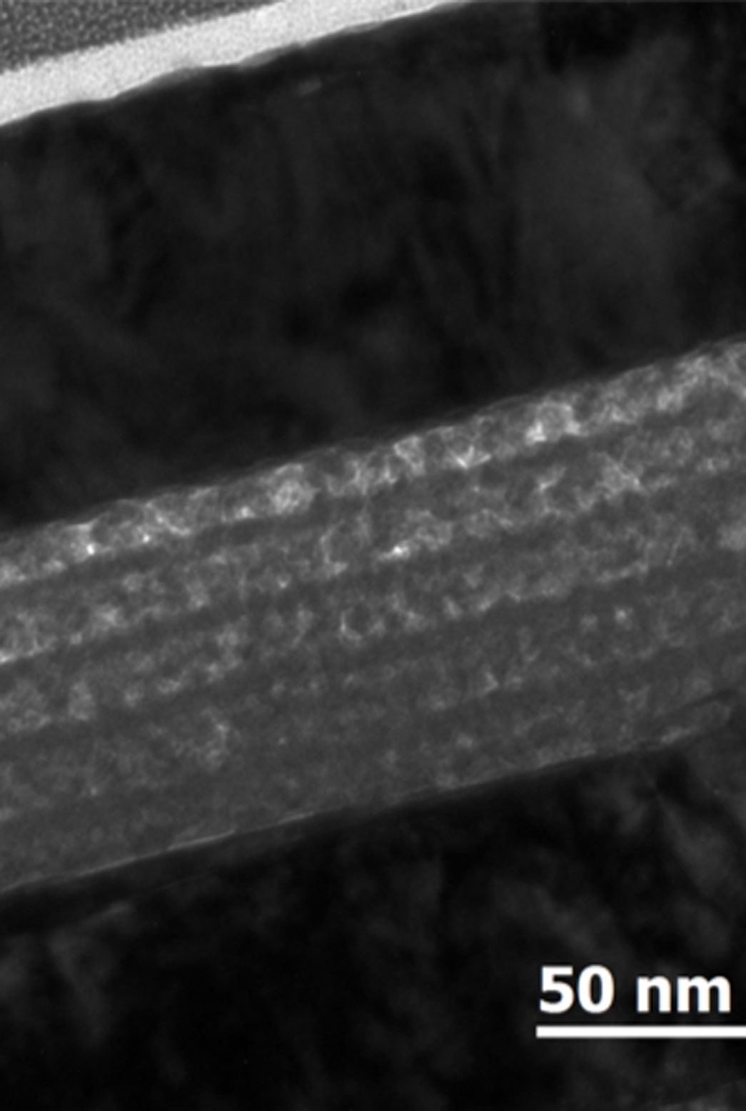
Peterson’s team managed this by using a different kind of semiconductor, known as an amorphous metal oxide. To apply this semiconductor layer to the silicon chip without damaging it, they covered the chip with a solution containing zinc and tin and spun it to create an even coat. Next, they baked the chip briefly to dry it. They repeated this process to make a layer of zinc-tin-oxide about 75 nanometers thick – about one thousandth the thickness of a human hair. During a final bake, the metals bonded to oxygen in the air, creating a layer of zinc-tin-oxide.

 Enlarge
The team used the zinc-tin-oxide film to make thin film transistors. These transistors could handle higher voltages than the silicon beneath. Then, the team tested the underlying silicon chip and confirmed that it still worked.
To make useful circuits with the silicon chip, the zinc-tin-oxide transistors needed to fully communicate with the underlying silicon transistors. The team accomplished this by adding two more circuit elements using the zinc-tin-oxide: a vertical thin film diode and a Schottky-gated transistor.
The two kinds of zinc-tin-oxide transistors are connected together to make an inverter, converting between the low voltage used by the silicon chip and the higher voltages used other components. The diodes were used to convert wireless signals into useful DC power for the silicon transistors. These demonstrations pave the way toward silicon integrated circuits that go beyond Moore’s law, bringing the analog and digital advantages of oxide electronics to individual silicon transistors.
This work was performed primarily by PhD student Youngbae Son (PhD Electrical and Computer Engineering 2019), with assistance from undergraduate researchers Brad Frost (BSE Electrical Engineering and BSE Computer Science Engineering 2016) and Yunkai Zhao (BSE Electrical Engineering 2015, MS Electrical Engineering 2016).
The paper is titled, “Monolithic integration of high-voltage thin-film electronics on low-voltage integrated circuits using a solution process.”
The study was funded by a Defense Advanced Research Projects Agency Young Faculty Award. The devices were fabricated in the Lurie Nanofabrication Facility.