Semiconductor workforce program increases access to hands-on training

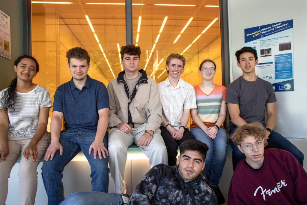
In a program designed to help grow the U.S. semiconductor workforce, a cohort of college students from across the country are spending summer at the University of Michigan learning how to make, study and improve advanced semiconductors.
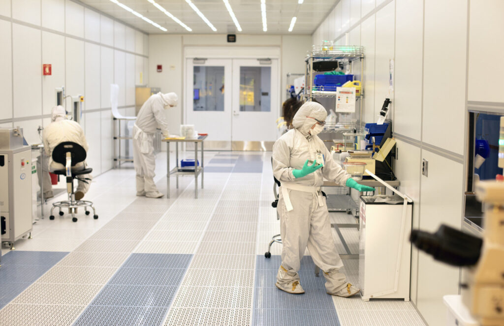
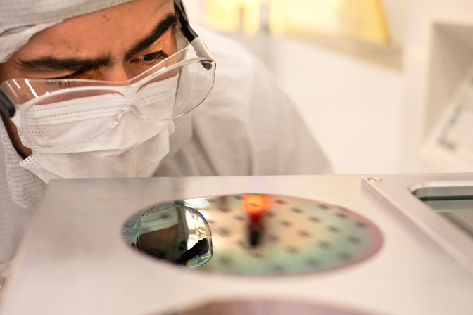
They’re working in the Lurie Nanofabrication Facility‘s world-class cleanroom, using industry-standard equipment, and immersing themselves in cutting-edge research. But no prior knowledge of nanofabrication was required for the 10-week Michigan Semiconductor Hands-On Research Experience, which is funded for three years by the National Science Foundation, with support from the Semiconductor Research Corporation. M-SHORE is designed to broaden participation in semiconductor-related engineering and encourage participants to pursue further academic studies in the field.
“The goal is to reach students who don’t have access to a facility like the Lurie Nanofabrication Facility or who have never had this type of hands-on training,” said Becky Peterson, an associate professor of electrical and computer engineering and director of the Lurie Nanofabrication Facility. “We want them to gain real experience making and testing devices in a lab—to go beyond putting together circuits in a class to building the physical layers that make the devices inside a cleanroom.”

Semiconductors are at the core of modern society, from our phones, tablets and computers, and the data center servers that form the internet, to cars, airplanes, robotic systems and even the industrial equipment used to manufacture these items. The recent chip shortage highlighted the need for the U.S. to expand the domestic semiconductor manufacturing industry and workforce.
“We need to focus on providing better training and expanding the number and types of students we train, so we can grow the workforce in this field in the United States,” Peterson said.
The students will work with U-M faculty and graduate students on projects in three areas:
Understanding and improving the performance of advanced semiconductor gallium nitride, or GaN, which belongs to a “wide bandgap” class that is critical to power electronics and clean energy. (A material’s bandgap is a measure of the amount of energy needed for electrons to be excited into states where they can contribute to an electric current.) Students are part of teams working to improve artificial photosynthesis systems that split water to produce hydrogen fuel, and to develop high-frequency and high-power transistors capable of supporting 6G networks and beyond.
Developing new nanofabrication methods to make materials and devices that address energy conversion and sustainability. Students are part of research teams making transparent aerogels that convert solar energy into heat, making mixed aerogel-nanoparticle paints that are pigment- and dye-free, and making ultrasensitive probes that can measure temperature and heat flow at the nanometer spatial scale. Aerogels are solid, porous foams made of interconnected nanostructures.
Investigating the behavior of complex oxide materials and devices—contenders to replace or augment silicon in computing, data storage, energy and sensing applications. Students will be part of teams using nanomanufacturing tools to synthesize and study advanced oxide materials, including entropy-stabilized complex oxides that can be used for multimodal devices; ultrawide bandgap oxide semiconductors that can be used for high voltage, high power future applications; and memristor memory chips that can store and process data at the same time.
Eyo Achamyeleh, who studies electrical engineering at Union College in New York, is working on one of the gallium nitride projects.
“We have learned about these devices, but now we’re learning how to actually make them,” Achamyeleh said. “I had never thought about how they’re made or what type of elements are in them. It was a whole different subject and language for me.”

Allan Flores, a senior at California State University, San Marcos, is studying applied physics, said the experience is leading him to consider a Ph.D., which would be a first in his family.
“My home institution is smaller and less focused on research,” he said. “In undergrad, you sometimes feel like you’re just passing classes. But what we’re doing here is science.”
This year, the student participants come from Embry-Riddle Aeronautical University; Union College; Sierra College; California State University, San Marcos; Purdue University-Fort Wayne; State College of Florida; Case Western Reserve University; and Trine University.
Going forward, U-M will work in partnership with two minority-serving institutions, the University of Texas at El Paso and Florida International University, to recruit participants and design collaborative projects.
U-M’s Lurie Nanofabrication Facility supports advanced semiconductor research, education and regional economic development. Faculty members, students, other institutions, national labs and industry use it for R&D, training and small-scale manufacturing. Over the past five years, the LNF has supported more than 900 users, including 95 companies, 150 U-M faculty members and researchers from 40 other U.S. universities and four international entities.
The effort is supported through the NSF Research Experiences for Undergraduates program in partnership with the Semiconductor Research Corporation.
Written by Hayley Hanway and Nicole Casal Moore