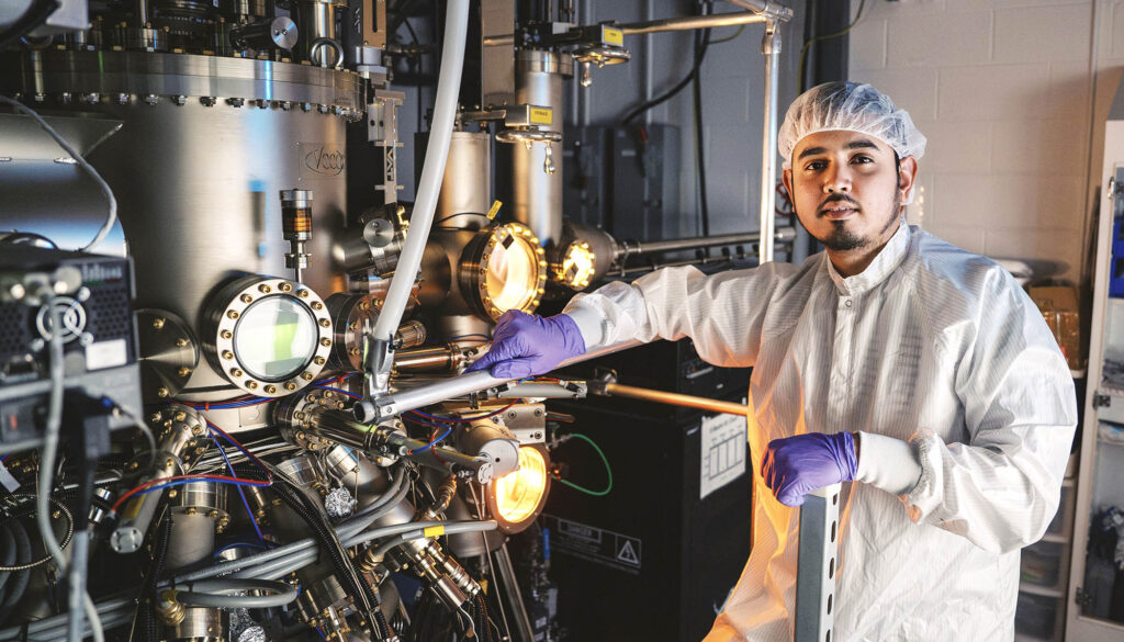
Shubham Mondal receives SVCF Scholarship to support his research in semiconductor materials

Shubham Mondal, an ECE PhD student, has been awarded a scholarship from the Society of Vacuum Coaters Foundation (SVCF) to support his research using III-Nitride based semiconductor materials to improve the operation of electronic and optoelectronic devices.
“Moving forward with my extensive experience in high-vacuum, thin film deposition technologies and semiconductor processing, I wish to drive meaningful advancements in emerging technologies, leading impactful projects to create solutions for the most pressing problems of the semiconductor industry,” Mondal said.

Mondal specializes in semiconductor processing and the epitaxial growth of III-Nitride thin films by Plasma Assisted Molecular Beam Epitaxy (PAMBE).
“In my forthcoming PhD research, I aim to address the long-standing challenge of p-doping in the epitaxy of N-polar wide bandgap III-Nitrides and make significant advances in the development Aluminum Gallium Nitride channel N-polar HEMTs on the Silicon Carbide platform,” Mondal said.
Mondal’s previous research accomplishments include:
- Contributing to the first demonstration of epitaxial growth and controllable doping in an N-polar wide-bandgap semiconductor, AlGaN (Aluminum Gallium Nitride), directly on the Silicon Carbide (SiC) substrate
- Demonstrating the practical utility of (Sc,Y) alloyed III-Nitrides, elucidating the crucial function of polarization switching in FeFETs for integrated memory-logic functionalities, along with exhibiting the versatility of ferroelectric III-Nitrides through self-powered, reconfigurable deep ultraviolet photodetectors
Mondal is advised by Prof. Zetian Mi, and he has co-authored 25 journal publications, five of which he first authored. He already received the 2023 APL Materials Excellence in Research Award.
Mondal is also pursuing a dual degree graduate certificate in Innovation and Entrepreneurship from the Center for Entrepreneurship. He earned his bachelor’s degree in ECE from Kalyani Government Engineering College, India. He is currently a member of Tau Beta Pi (the Engineering Honor Society) and Eta Kappa Nu (the ECE Honor Society), and he is a board member for the ECE Graduate Student Council.